TECHNOLOGY IN THE LNQE RESEARCH BUILDING


In the LNQE research building, equipment and technologies are made available centrally to employees and students from the working groups and institutes of the Leibniz Research Center LNQE.
Lithography
-
Photolithography for silicon and germanium
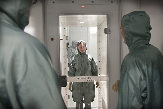
- The cleanroom has an ISO 5 cleanroom class.
- UV contact and proximity exposure units for round wafers (silicon and germanium) up to 100 mm diameter. Mask size 150*150 mm2 square, minimum line width 900 nm (SÜSS MA 150 and MA 6)
- UV manual exposure for fragments and small wafers
- Spin coater with heating plate for round wafers up to 200 mm diameter. Heating up to 200°C (SÜSS DELTA 80 and LABSPIN 8 )
- Spraycoater AS8
- Drying oven for vapour deposition on adhesion promoters
- Hotplate HP8TT
- HMDS Hotplate VP8 T/BM
- Plasma Asher for round wafers up to 100 mm diameter, for removing resist residues in O2 plasma (TEPLA 100 and GIGAbatch 360M )
- Wet benches for ultrasonic development and resist removal
- Refrigerators for resist chemistry
![]()
![]()
![]()
-
Photolithography for all other materials
- The cleanroom has an ISO 5 cleanroom class.
- UV contact and proximity exposure units for round wafers (compound semiconductors) up to 100 mm diameter. Mask size 150*150 mm^2 square, minimum line width 700 nm (SUSS MA6)
- Spin coater with heating plate for round wafers up to 100 mm diameter. Heating up to 200°C (SÜSS LABSPIN 6)
- Wet benches for development and resist removal
![]()
![]()
![]()
-
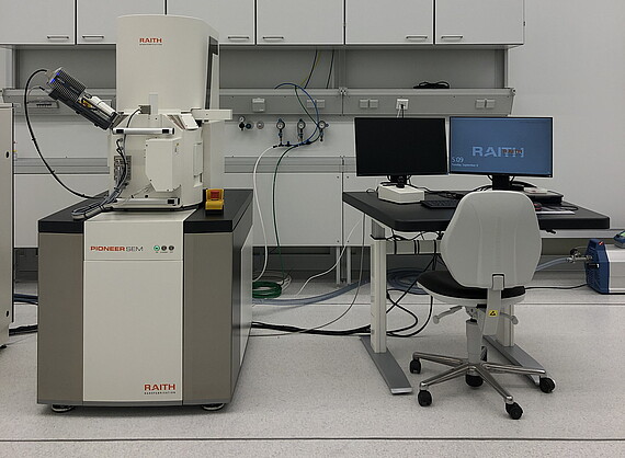
Hybrid system for electron beam lithography and scanning electron microscopy (EBL-SEM)
The Pioneer Two system in the LNQE research building is a hybrid system for electron beam lithography and scanning electron microscopy (EBL-SEM). It has a maximum acceleration voltage of 30 kV and uses as an electron emitter a thermal field emission (TFE) Schottky-source. The most important parameters are:
- System type: Pioneer Two from Raith
- Beam current: 5pA – 20 nA, beam size: < 1,6 nm
- Inlens detector, dual-detector for secondary and backscattered electrons
- EDX–detector (Bruker QUANTAX 200) for elements between Z=5 and Z=95
- Nanolithography resolution: 8 nm
- Pattern generator speed: 6 MHz
- Field stitching und overlayer accuracy: 50 nm
- Stage travel range: 50 x 50 x 25 mm
- Stage with 360° rotation und 0 – 90°tilt
Use:
- Terms of Use ESL-REM
- Contakt: Mr. Chenxi Ma (Group Ding), c.ma@fkp.uni-hannover.de, +49 511 762 14448
![]()
![]()
![]()
-
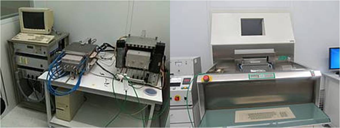
Scanning electron microscope with e-beam lithography
- Jeol JSM-5900 SEM
- E-Beam writing with Raith Elphy plus
![]()
![]()
![]()


Etching
-
Wet benches
Wet benches for wet-chemical structuring and cleaning of round wafers up to 200 mm diameter (also solar)
- Piranha and RCA cleaning (SC1, SC2, HF-Dip)
- Quick dump rinser
- Spin rinser dryer
- Wet chemical etching processes in general
![]()
![]()
![]()
-
Reactive Ion Etching (RIE)
Reactive ion etching for round wafers up to 100 mm diameter, etching under Ar, O2, SF6 and CHF3 (ALCATEL RIE)
![]()
![]()
![]()
Device for Reactive Ion Etching (RIE) with Inductive Coupled Plasma (ICP) Source for Cl and F chemistry (OXFORD RIE).
RIE technique combines isotropic chemical etching and anisotropic physical etching (sputtering).
- RIE: control on ion energy and ion density, but not independently.
- ICP: control on ion density
- ICP-RIE: independent control on ion density and ion energy.
![]()
![]()
![]()


Ion Implantation
-
Ion implanter
Ion implanter for round wafers up to 300 mm diameter, also Solar, As, P, B, 5-60 keV (VARIAN VIISta HC)
![]()
![]()
![]()


Oxidation and Layer Deposition
-
Vertical furnace system
Vertical furnace system for wet and dry oxidation of silicon up to 150 mm diameter, up to 1100 °C (CENTROTHERM VERTICOO 200)
Verticoo 200 vertical furnace system from Centrotherm, oxidation tube, vertical, oxidation dry and moist, moist oxidation with steamer (steam from DI water) or hydrox burner (steam from H2 and O2 burned). Disc size 150 mm and 200 mm, with adapters also 100 mm and "pieces", full handling system, but also manually operable. All oxidation tubes are equipped with a DCE bubbler.
![]()
![]()
![]()
-
Horizontal cluster system
Horizontal cluster system for silicon up to 200 mm diameter, also solar: (CENTROTHERM EUROPE 2000)
- Top: SiC tube up to 1285 °C, dry and moist oxidation, moist oxidation with steamer (steam from DI water) or hydrox burner (steam from H2 and O2 burnt).
- Below: Polysilicon tube, doped and undoped, amorphous and polycrystalline, n and p doped with phosphine and diborane and with oxygen as SIPOS.
- Below: Nitride tube, stoichiometric (Si3N4) and Si-rich nitride with low stresses, i.e. "low-stress nitrides" can be produced (compressive and tensil layer stress).
- Below: LPCVD-TEOS tube, low-temperature oxides, with plasma support, temperatures from 450 °C.
All tubes designed for 200 mm, boats for rectangular solar wafers, round 150 mm and 100 mm as well as 2" and 3" available. All oxidation tubes are equipped with a DCE bubbler to enable high temperature cleaning with chlorine. This achieves good freedom from metal ions.
![]()
![]()
![]()
-
Plasma CVD
Plasma-CVD for round wafers up to 100 mm diameter, production of oxides, nitrides, poly and germanium, substrate temperature up to 400 °C (OXFORD PLASMALAB 90)
![]()
![]()
![]()


Metallization
-
Evaporation coating system
HHV Thin Film Deposition System ATS 500 - Evaporation
- Telemark multi pocket electron beam evaporation source
- 6 crucibles of 7 cc volume each (used with 4cc liners)
- 270° beam deflection
- 6kW power rating
- X-Y beam sweep coils
- Plug-in emitter assembly
- Ultimate vacuum < 2 x 10⁻⁷ mbar
- Sample holder up to 6” wafer
- 360° sample rotation, variable rotation speeds in the range 20 to 60 RPM
- Quartz lamp substrate heater up to 250 °C
- Film thickness measurement via quartz crystal sensor
- Evaporation materials (for the moment): Au, Ti, Cr, Ni, Ge, SiO2
Usage: Ankita Choudhary, (Group Zopf), ankita.choudhary@fkp.uni-hannover.de
![]()
![]()
![]()
Evaporation coating system for round wafers up to 100 mm diameter, 4-fold crucible and single crucible, co-evaporation (BALZERS BAK 610)
![]()
![]()
![]()
-
Cathode sputtering system
HHV Thin Film Deposition System ATS 500 - Sputtering
- DC and RF magnetron sputtering
- up to 1.5 kW DC power
- up to 600 W RF power at 13.56 MHz
- Four target holders
- With load lock chamber
- Max. four inch substrates -rotating workpiece holder (0 to 60 rpm)
- Workpiece holder with "flip" mechanism -Manual and automatic process mode
- Process gases: argon, nitrogen, oxygen -Substrate heating up to 700 °C
- Glow discharge cleaning of the substrate before process possible
Usage: Jacob Stupp (Group C. Ospelkaus), stupp@iqo.uni-hannover.de, +49 511 762 16055
![]()
![]()
![]()
LEYBOLD Z590
- DC and RF magnetron sputtering with up to 5kW DC power with up to 2.5kW RF power
- Four target holders, loading via load lock chamber
- Max. 200mm substrates rotating under the targets with homogeneity baffles
- Manual and automatic process mode
- Process gases: argon, nitrogen, oxygen
- Substrate heating up to 700 °C
- Plasma etching up to 2.5kW
- Liquid nitrogen cooling trap
![]()
![]()
![]()
-
Resistive evaporator
Resistance evaporator "Congo Vac" for vapour deposition of wafers and small pieces with gold, titanium, and other metals (chromium, germanium, silver, aluminium, nickel, lead, indium, palladium, niobium, hafnium, copper)
Usage: Jacob Stupp (Group C. Ospelkaus), stupp@iqo.uni-hannover.de, +49 511 762 16055
![]()
![]()
![]()


Annealing
-
Rapid thermal processing
Rapid thermal processing at normal pressure, for round wafers up to 150 mm diameter, also solar, tempering up to 1100 °C under Ar, O2, N2 or N2H2. (AST SHS 2000 and self-made)
![]()
![]()
![]()
-
Polyimid oven
Bis 100 mm Durchmesser, Tempern unter Ar, N2 oder im Feinvakuum, bis 950 °C, rezeptgesteuert.
![]()
![]()
![]()


3D Printing
-
Selective laser-induced etching
LightFab 3D Printer M with IR Laser 1030 nm
- Subtractive manufacturing of glass substrates using selective laser-induced etching (SLE).
- Two-step process:
- Illumination of the substrate using fs laser to increase the local etchability of the material (LightFab 3D Printer).
- Removal of the illuminated structures using KOH solution in an ultrasonic bath.
- Machinable materials: including fused silica, sapphire, borosilicate glass, aluminosilicate glass, quartz, diamond.
- 3D structures up to a precision of ~1 µm possible.
- Suitable for substrates up to 200 mm in diameter. Material height or structure depth is material dependent.
- The system can additionally and in combination realize laser welding, laser ablation and 2-photon polymerization.
Usage:
- Contact: Jacob Stupp (C. Ospelkaus Group), stupp@iqo.uni-hannover.de, +49 511 762 16055
![]()
![]()
![]()


Wire bonding
-
Wire bonder
Wedge & Ball Bonder with motorized z and x axis, Ribbon is also possible.
It has easy operation with TFT touch screen with direct access and easy setting of all bonding parameters. It can be bonded with gold and aluminum wires (HB16 Wedge & Ball Bonder tpt).
![]()
![]()
![]()


Analytics
-
Spectral ellipsometer
The spectral ellipsometer is characterised by simple operation, measuring speed and combined data analysis of ellipsometric measurements at different angles of incidence (40-90°). It measures in the spectral range from 250 nm to 800 nm. The spectral range of the Sentech SE800 in combination with the SpectraRay/4 software makes it easy to determine, for example, the thickness and refractive index of individual layers through to complex layer stacks. Ready-to-use application files make operation very easy, even for beginners. The ellipsometer supports computer-controlled mapping for homogeneity measurements of samples up to 200 mm in diameter. Both extremely thin layers of 1 nm and - with sufficient transparency - thick layers of up to 15 μm can be measured.
![]()
![]()
![]()
-
Wafer probe station
Wafer probe station for round wafers up to 200 mm diameter (also solar), -65 °C to +200 °C sample temperature, digital camera system, 4 measuring needles (CASCADE SUMMIT 11000). With Impedance Analyzer (Agilent 4294A) and Semiconductor Parameter Analyzer (HP 4155).
![]()
![]()
![]()
-
Four-point measuring station
Four-point measuring station for measuring the layer resistance of a wafer (max. 200 mm diameter, all shapes) according to the measuring principle of four-point measurement. It can be measured manually at selected points on the wafer, or automatically according to a defined pattern and distance.
![]()
![]()
![]()
-
Confocal microscope
Confocal microscope with Mirau interferometer, up to 1500x magnification, height resolution up to 1 nm (LEICA DCM 3D)
![]()
![]()
![]()
-
Digital microscope
Digital microscopes (Keyence VHX 7000N)
- 4K CMOS camera
- Motorised stage for XYZ directions
- Tilt angle +60°to -90°, whereby the object remains in the centre
- Objectives in the motorised turret:
- 20-100x, lateral 4µm, Z 6µm resolution limit
- 100-500x, lateral 1.2µm, Z 1.5µm resolution limit
- 500-2500x, lateral 0.25µm, Z 0.4µm resolution limit
![]()
![]()
![]()
-
Digital Holographic Microscope
Digital Holographic Microscope (LyncéeTec DHM-R2104)
- Reflection DHM
- Resolution down to the nanometre range
- Measurement of dynamic processes up to 25 MHz
- High speed camera
- Stroboscopic module
- Vacuum option
- 2 laser sources
- Precision sample stage
- Multiple objectives
- Comprehensive software (capture + analysis)
Usage: Ioannis Lampouras (Group Körner), lampouras@geml.uni-hannover.de
![]()
![]()
![]()
-
Atomic force microscope (AFM)
Atomic Force Microscope (Nanosurf CoreAFM)
Easy-to-use AFM for research.
Measuring modes:
- Static Force Microscopy
- Lateral Force Microscopy
- Standard Spectroscopy
- Standard Lithography
- Dynamic Force Microscopy
- Phase Contrast Microscopy
- Force Modulation Mode
- MFM
- Liquid Imaging
- „QuickPrescan“, Up to 8 times faster and tip-saving image previews
- Kelvin Probe Force Microscopy (KPFM)
- Piezoresponse Force Microscopy (PFM)
![]()
![]()
![]()
-
Tactile Profilometer
Tactile Profilometer (Bruker DektakXT-A)
- Tactile measurements of step height, layer thickness, depth of structures incorporated into substrates, and surface finish characterization.
- Measurement range 1,000 μm down to 10 nanometers with accuracy down to 0.4 nanometers.
- 3D mapping on a motorized stage with rotatable 200 mm vacuum chuck.
Usage: Jacob Stupp (Group C. Ospelkaus), stupp@iqo.uni-hannover.de, +49 511 762 16055![]()
![]()
![]()
-
Scanning electron microscope with e-beam lithography
- Jeol JSM-5900 SEM
- E-Beam writing with Raith Elphy plus
![]()
![]()
![]()
-
Transmission electron microscope (TEM)
The TEM in the LNQE has an acceleration voltage of 200 kV and as an electron emitter a field effect cathode. The most important parameters are:
- Device type: TEM Tecnai G2 F20 TMP from FEI
- 200 kV Field effect FEG
- OBJECTIVE LENS TYPES: TWIN
- Oil-free vacuum
- TEM point resolution: 0.27 nm
- Information limit: 0.14 nm (measured)
- STEM resolution: 0.24 nm
- 1 brightfield and 2 darkfield detectors +1 HAADF detector
- Tomography +- 70° (possibly up to +- 80°)
- EDX-Detektor (EDAX Octane T Optima 60 SDD System)
With this TEM all classical contrast methods are possible: bright field and dark field, diffraction contrast (including weak beam), parallel illumination at all magnifications (especially important for the examination of crystalline samples), TEM and STEM (scanning TEM). Large tilting angles are possible. A special feature of the TEM in the LNQE is the possibility of tomography.
For sample preparation, a Gatan PIPS 691 ion polishing system, Gatan Dimpler Grinder 656, light microscopes, fume hood and small laboratory equipment are available.
Contact to the TEM:
Dr. Fritz Schulze-Wischeler, Schulze-Wischeler@LNQE.uni-hannover.de, Tel.: +49 511 762 16014![]()
![]()
![]()
![]()
![]()
![]()
-
X-ray photoelectron spectroscopy (XPS)
X-ray photoelectron spectroscope (XPS) for non-destructive determination of chemical composition, primarily of solids or their surfaces.
Equipment features:
- PHI Versaprobe III Scanning ESCA
- Heatable and coolable sample chamber
- UPS option
- LEIPS Option
- Scanning Auger Option
- Gas Cluster Ion Source
Usage:- XPS usage regulations (GE)
- Contact: Dr. Andreas Schaate (andreas.schaate@acb.uni-hannover.de, +49 511 762 3698)
![]()
![]()
![]()


Contact to Technology


30167 Hannover