
TECHNOLOGY IN THE LNQE RESEARCH BUILDING
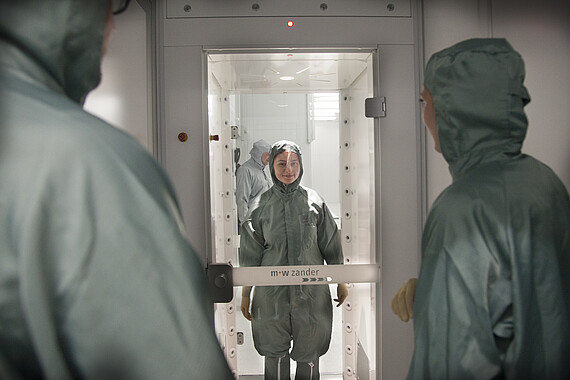


In the LNQE research building, equipment and technologies are made available centrally to employees and students from the working groups and institutes of the Leibniz Research Center LNQE.


Ion Implantation


Oxidation and Layer Deposition


Annealing


3D Printing


Assembly


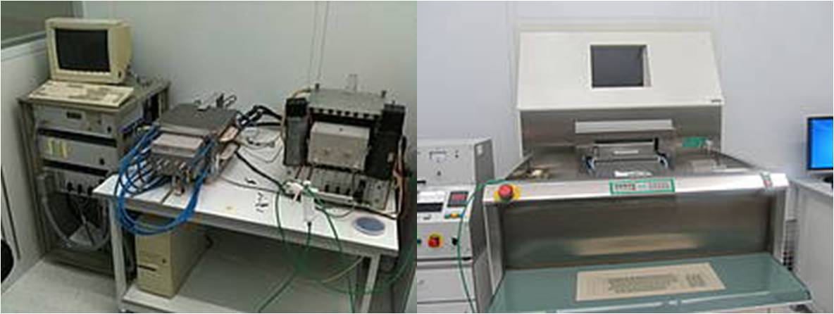
Analytics
- Spectral ellipsometer
- Wafer probe station
- Four-point measuring station
- Confocal microscope
- Digital microscope
- Digital Holographic Microscope
- Atomic force microscope (AFM)
- Tactile Profilometer
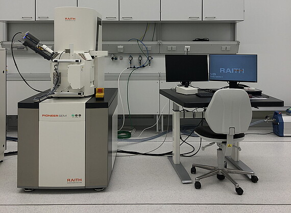
- Scanning electron microscope with e-beam lithography
- Transmission electron microscope (TEM)
- X-ray photoelectron spectroscopy (XPS)


Contact to Technology

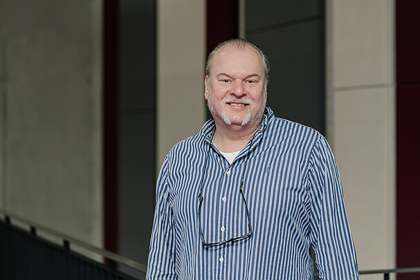
Dipl.-Ing. Oliver Kerker
Chief Technical Officer
Phone
Address
Schneiderberg 39
30167 Hannover
30167 Hannover
Building
Room
Dipl.-Ing. Oliver Kerker
Chief Technical Officer


![[Translate to English:] Logo Zusammenland farbig](/fileadmin/_processed_/a/9/csm_zusammenland_4c_e78505eb7d.png)
![[Translate to English:] Logo Zusammenland-schwarzweiß](/fileadmin/_processed_/1/2/csm_zusammenland_sw_f06954e75c.png)