Cryogenic Delta-Sigma Analog-to-Digital Converter for Spin-Qubit State Readout
| Led by: | Supervisor: Prof. Dr.-Ing. Pascal Witte, University of Applied Sciences and Arts in Hannover. Co-Supervisor: Prof. Dr.-Ing. Bernhard Wicht, LUH, Insitute of Microelectronic Systems |
| Team: | Jesko Flemming |
| Year: | 2022 |
Advancing quantum technology towards scalable clusters of qubits is challenging across all involved disciplines, such as physics, material sciences, electronics, computer science, and mathematics. A main focus in the field of electronics is on building efficient interface circuits, which allow a reliable readout and control of qubits. Amongst various technologies realizing qubits, superconducting and spin-based technologies are currently the most promising technologies for integration with state-of-the-art solid-state circuit technologies [1]. Furthermore, spin-based qubit technologies tend to allow an operation at temperatures slightly above 1 K. This again supports achievements to integrate electronic circuits together with qubits in the same location. One of the major challenges for integrating qubits and electronic circuits is the very limited power budget per qubit, due to physical limitations on cooling capabilities for cryogenic temperatures.
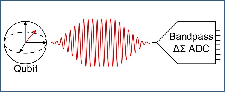
A promising circuit architecture to readout the state of a qubit is a Bandpass Delta-Sigma Analog-to-Digital Converter (BP ΔΣ-ADC), which uses subsampling to circumvent explicit down-conversion of the input signal. BP ΔΣ-ADCs allow a direct A-to-D conversion of the frequency band, without prior down-conversion of the input signal. This reduces the required analog front-end significantly and allows a low-power and high-resolution conversion of the signals of interest.
The goal of this PhD project is to build a cryogenic subsampling BP ΔΣ-ADC for reading out spin-based qubit states. Besides building the circuits for the ADC, the project involves identifying a suitable ADC configuration, an according semiconductor technology, building simulation models reflecting device characteristics at cryogenic temperatures, and testing the built and manufactured ADC.
The work will be conducted utilizing industry-standard design tools and high-end laboratory equipment.
Figure: Qubit, signal reflecting the state of the qubit, and bandpass ΔΣ-ADC
[1] A. Crippa u. a., „Gate-reflectometry dispersive readout and coherent control of a spin qubit in silicon“, Nat Commun, Bd. 10, Nr. 1, S. 1–6, Juli 2019, doi: 10.1038/s41467-019-10848-z.